*********************************************
Publication List of Yoshiaki Hagiwara
as of March 5, 2025
*********************************************
ダブル接合型太陽電池の提案_LOCOMTEC_萩原研究所_萩原良昭.jpg)
SONYのHADセンサー(Pinned_Photodiode)ダブル接合型太陽電池の提案.pdf
2025_02_13_LOCOMTEC_萩原AIPS研究所の活動紹介.pdf
2025_02_13_LOCOMTEC_萩原AIPS研究所の活動紹介.mp4
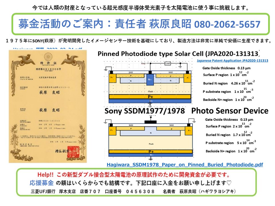
超光感度半導体受光素子を太陽電池に使う事に挑戦します_萩原良昭.pdf
C2025_02_23_シングルPN接合型太陽電池では空乏層幅は最大2μmが限界である事が簡単な計算で求まる_萩原良昭.pdf

C2025_02_22_シングルPN接合型太陽電池では空乏層幅は最大2μmが限界である事が簡単な計算で求まる_萩原良昭.pdf
+++++++++++++++++++++++++++++++++++++++++++++++++++++++++
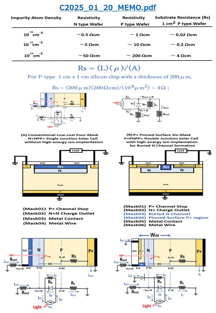
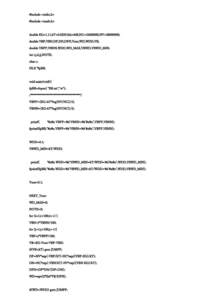
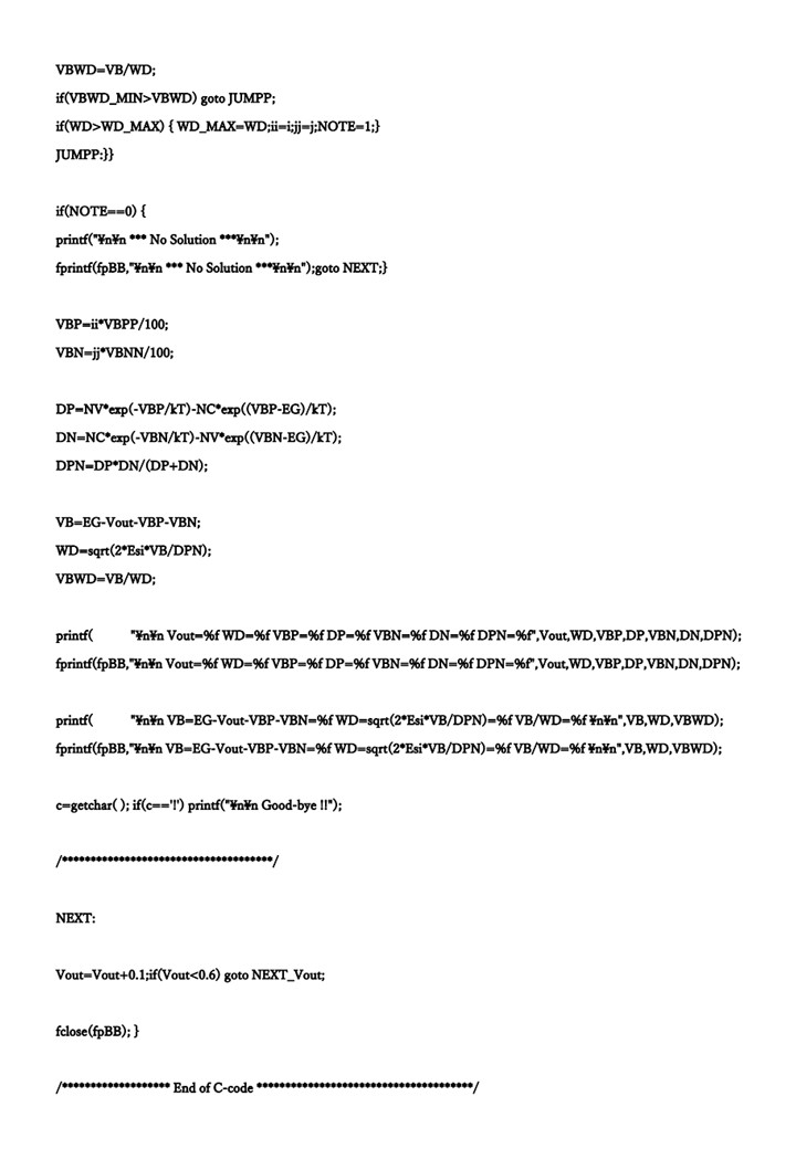
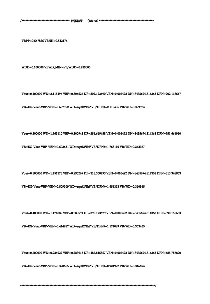
C2025_01_20_Memo_Solar_Cell.pdf
+++++++++++++++++++++++++++++++++++++++++++++++++++++++++
+++++++++++++++++++++++++++++++++++++++++++++++++++++++++
Pinned_Surface_Completely_Depleted_Buried_Channel_Double_Junction_type_Solar_Cell.pdf
01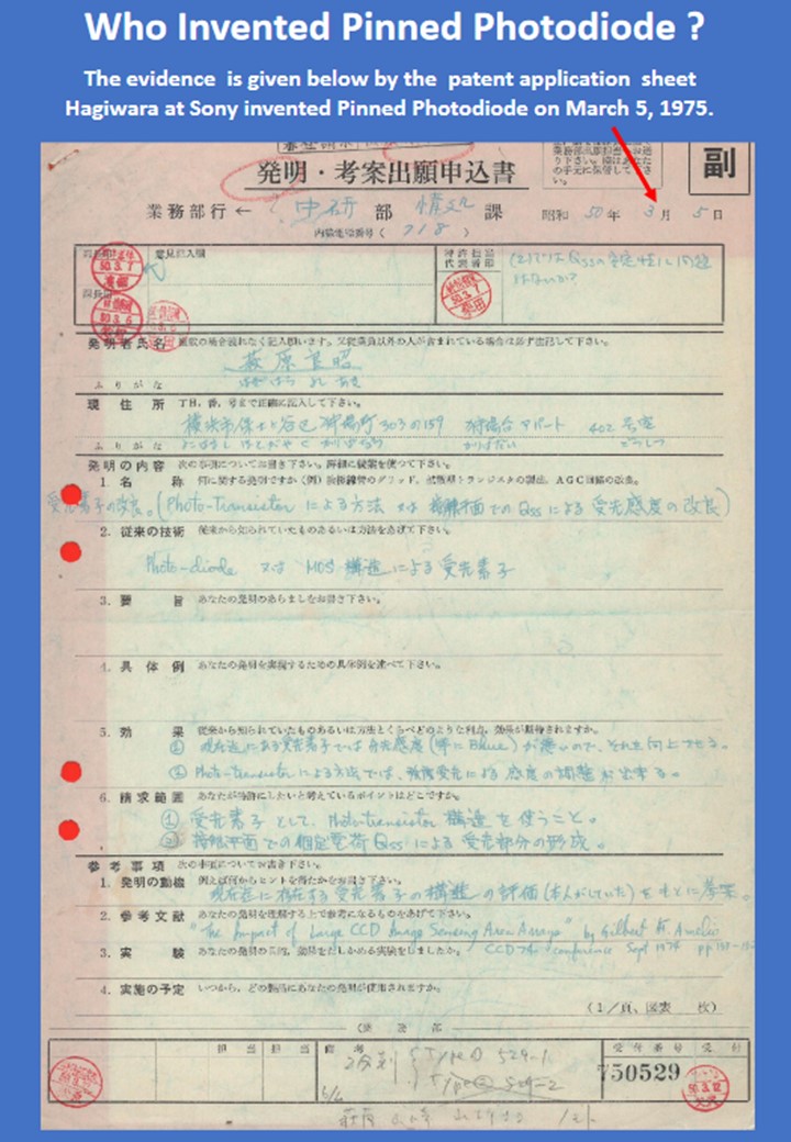
02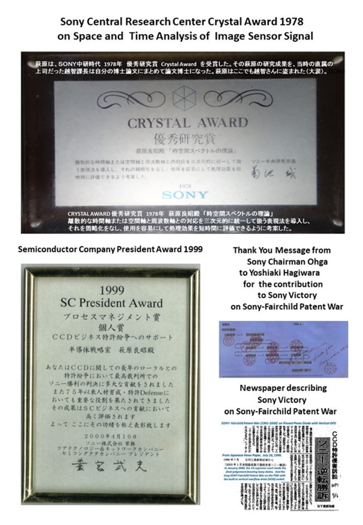
03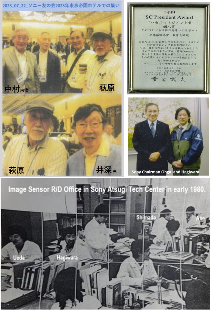
04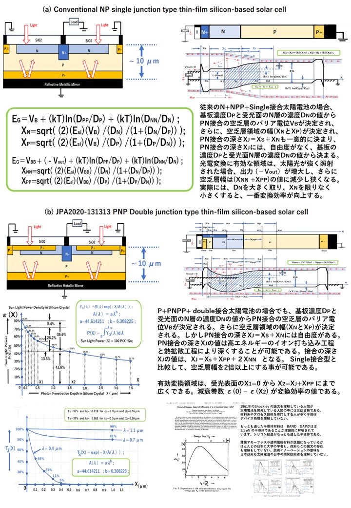
05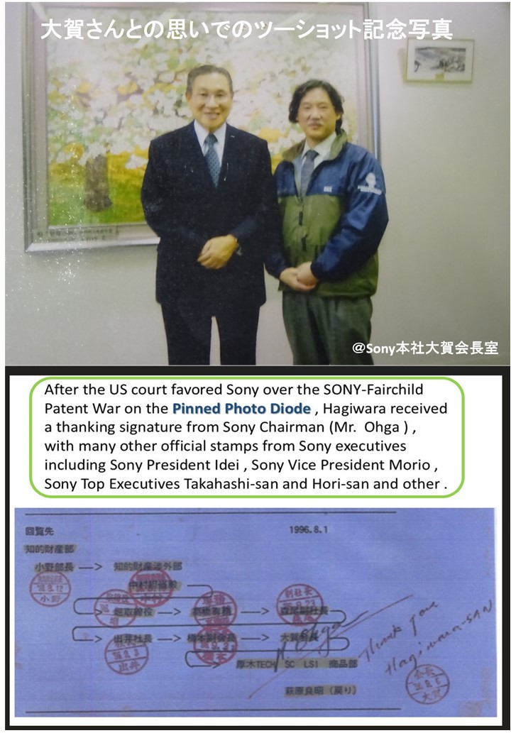
06
07
08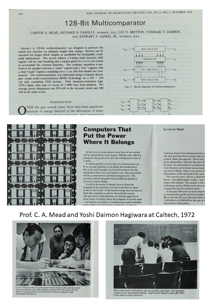
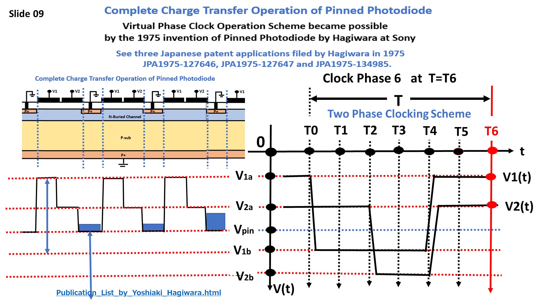
09
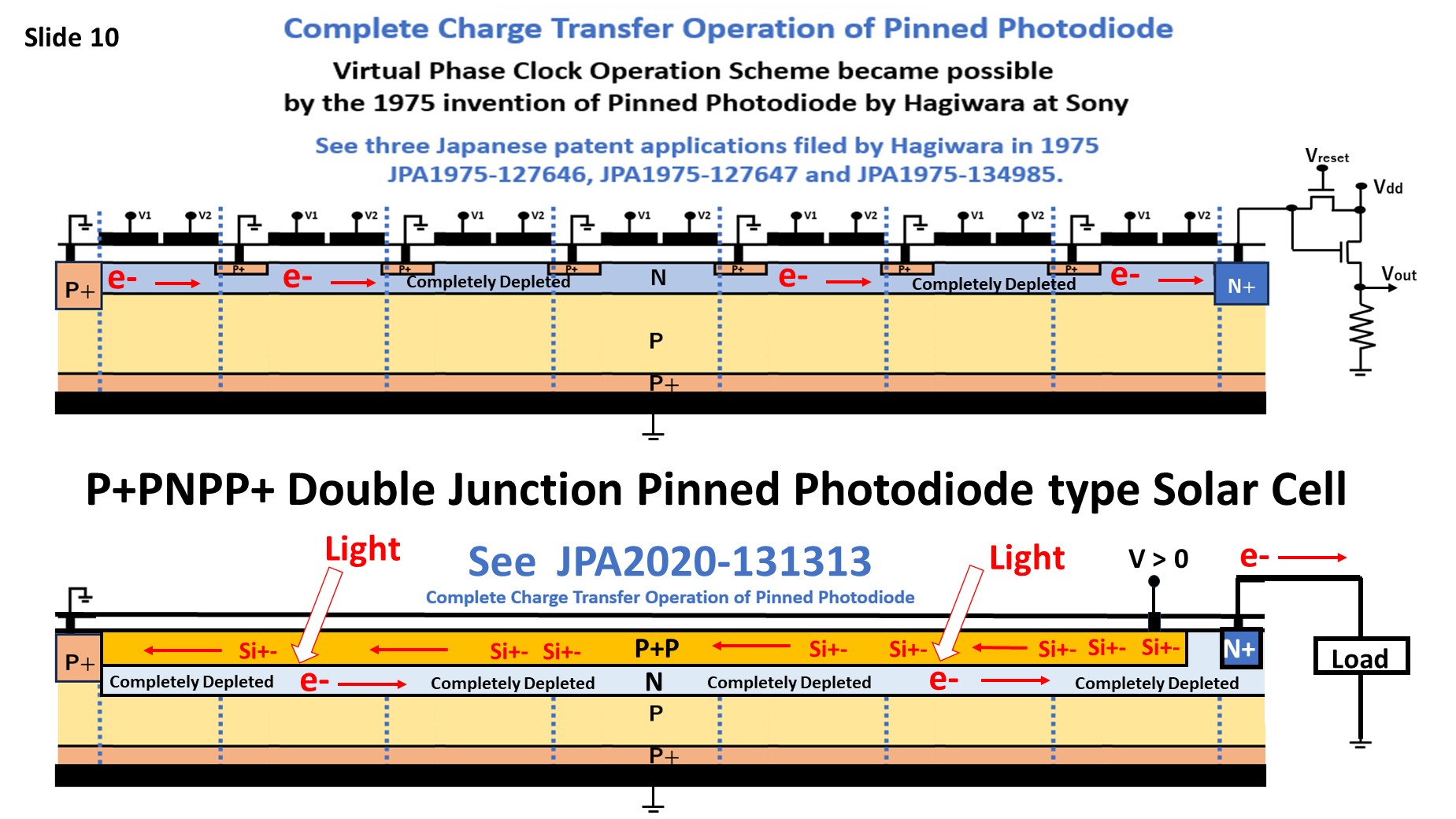
10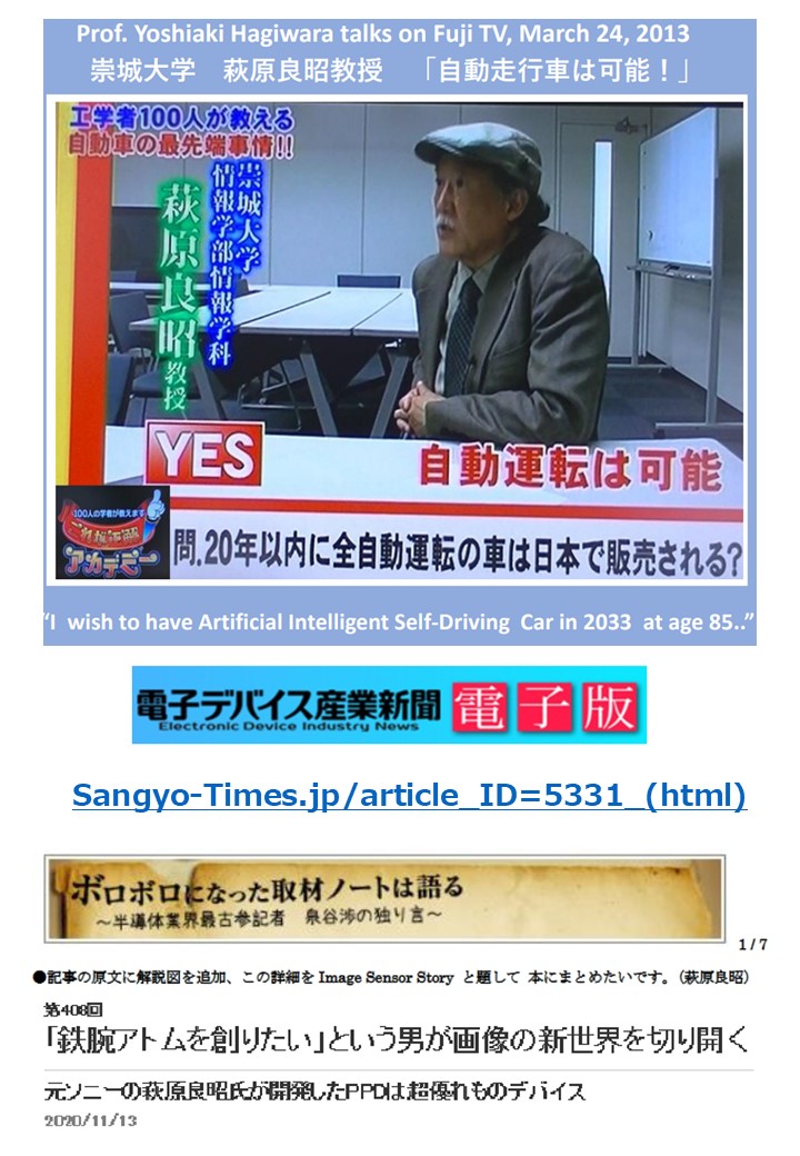
+++++++++++++++++++++++++++++++++++++++++++++++++++++++++
のLife_Work_夢と挑戦_1.jpg)
のLife_Work_夢と挑戦_2.jpg)
のLife_Work_夢と挑戦_3.jpg)
SONY(萩原良昭)のLife_Work_夢と挑戦.pdf
+++++++++++++++++++++++++++++++++++++++++++++++++++++++++
2025_02_11_良昭のひとりごと.mp4
+++++++++++++++++++++++++++++++++++++++++++++++++++++++++
C2025_01_23_Memo.pdf

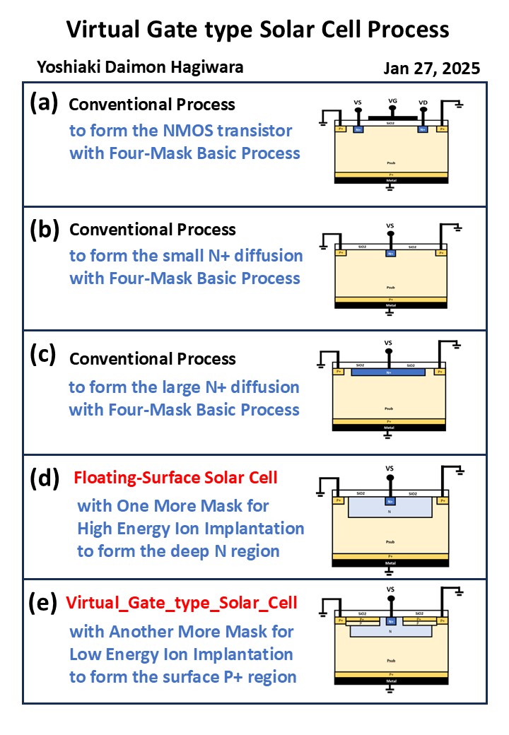
Virtual_Gate_type_Solar_Cell_Process_by_Yoshiaki_Daimon_Hagiwara.pdf
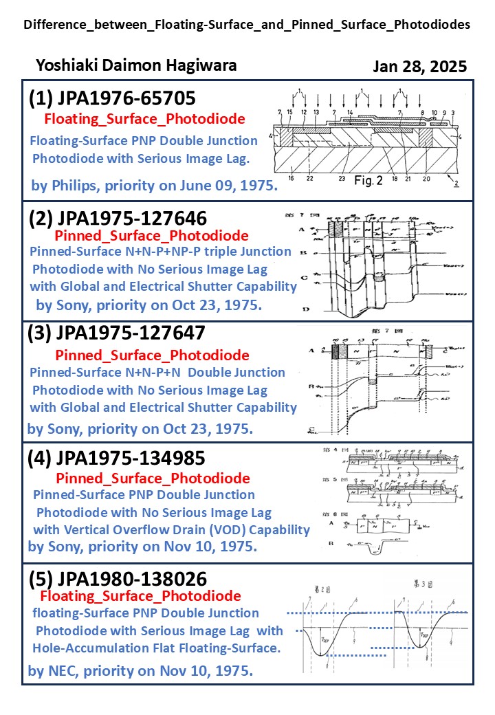
Difference_between_Floating-Surface_and_Pinned_Surface_Photodiodes_by_Yoshiaki_Daimon_Hagiwara.pdf
+++++++++++++++++++++++++++++++++++++++++++++++++++++++++
+++++++++++++++++++++++++++++++++++++++++++++++++++++++++
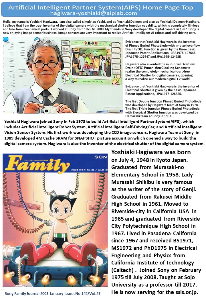
Bio_and_List_of_Publications_Yoshiaki_Daimon_Hagiwara.pdf
+++++++++++++++++++++++++++++++++++++++++++++++++++++++++
Smart_AI_Robot_Vision_Image_Sensor_also_works_as_Solar_Cell_Yoshiaki_Hagiwara.pdf
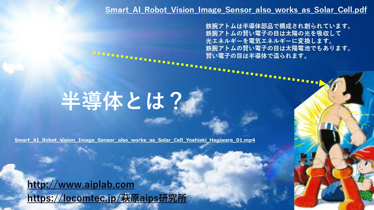
Smart_AI_Robot_Vision_Image_Sensor_also_works_as_Solar_Cell_Yoshiaki_Hagiwara_01.mp4
Concept_of_Electron_Fog_amd_Solar_Cell_Band_Diagram.pdf
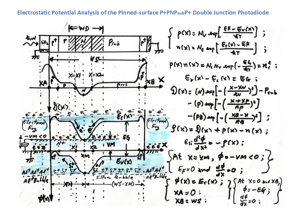
Electrostatic_Potential_Analysis_of_the_Pinned-surface_P+PNPsubP+_Double_Junction_Photodiode.pdf
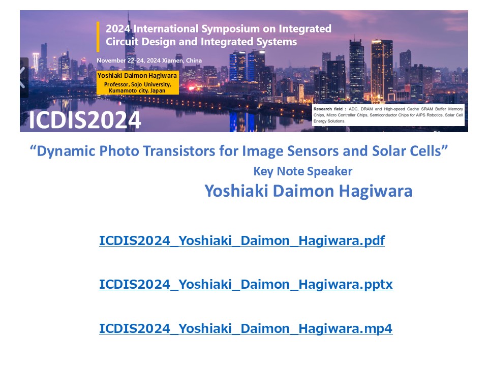
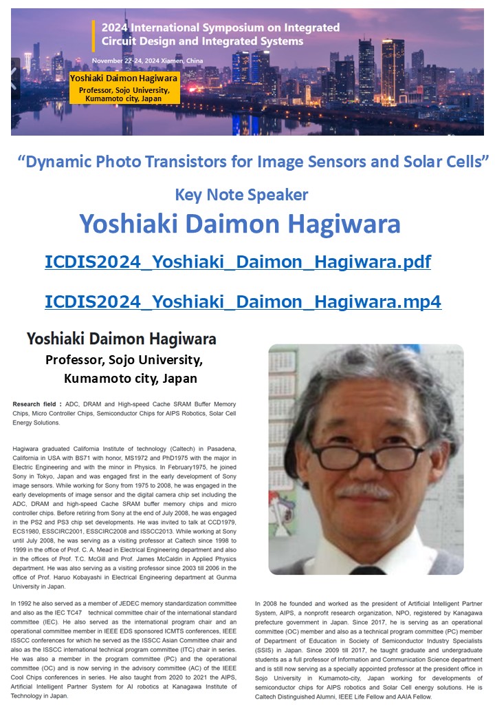
2024_11_22_ICDIS2024_Conference_Slides_Link_Hagiwara.pdf
++++++++++++++++++++++++++++++++++++++++++++++++++++++
Locomtec.jp/萩原aips研究所のご案内
+++++++++++++++++++++++++++++++++++++++++++++++++++++++++
Hagiwara_履歴_2023_03_24.pdf
++++++++++++++++++++++++++++++++++++++++++++++++++++++
Publication_List_by_Yoshiaki_Hagiwara.html
Hagiwara_履歴_2023_03_24.pdf
++++++++++++++++++++++++++++++++++++++++++++++++++++++
++++++++++++++++++++++++++++++++++++++++++++++++++++++
Back-ups AIPS Home Pages
++++++++++++++++++++++++++++++++++++++++++++++++++++++
AIPS_240822.html
AIPS_240309.html
AIPS_230316.html
AIPS_221231.html
AIPS_220823.html
AIPS_220131.html
AIPS_211226.html
AIPS_211206.html
AIPS_211107.html
AIPS_210929.html
AIPS_210906.html
AIPS_210811.html
AIPS_210404.html
AIPS_210301.html
AIPS_210217.html
AIPS_210215.html
AIPS_201209.html
AIPS_200627.html
AIPS_190925.html
AIPS_190712.html
AIPS_181129.html
AIPS_090628.html
+++++++++++++++++++++++++++++++++++++++++++++++++++++++++
+++++++++++++++++++++++++++++++++++++++++++++++++++++++++
https://www.sojo-u.ac.jp hagiwara(@)ofc.sojo-u.ac.jp
https://www.ssis.or.jp hagiwara(@)ssis.or.jp
http://www.aiplab.com hagiwara(@)aiplab.com
https://locomtec.jp/萩原aips研究所
https://ja.wikipedia.org/wiki/萩原良昭
https://en.wikipedia.org/wiki/Yoshiaki_Hagiwara
+++++++++++++++++++++++++++++++++++++++++++++++++++++++++
Return to Top Home Page of Yoshiaki Hagiwara (AIPS)
http://www.aiplab.com
+++++++++++++++++++++++++++++++++++++++++++++++++++++++++
++++++++++++++++++++++++++++++++++++++++++++++++++++++
2024_11_22_ICDIS2024_Key_Note_Yoshiaki_Daimon_Hagiwara_Sojo_University.pdf
+++++++++++++++++++++++++++++++++++++++++++++++++++++++++
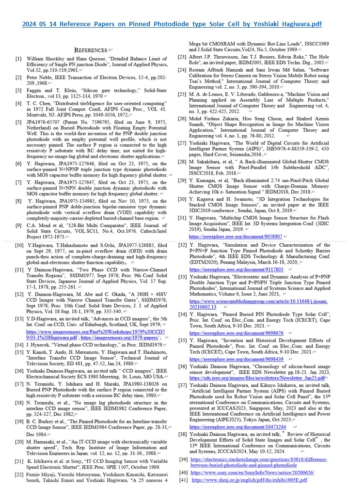
2024_05_14_Reference_Papers_on_Pinned_Photodiode_type_Solar_Cell_by_Yoshiaki_Hagiwara.pdf
+++++++++++++++++++++++++++++++++++++++++++++++++++++++++
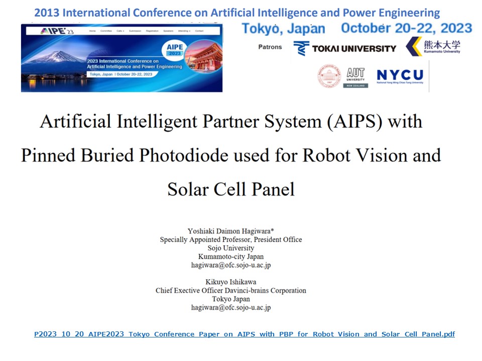
P2023_10_20_AIPE2023_Tokyo_Conference_Paper_on_AIPS_with_PBP_for_Robot_Vision_and_Solar_Cell_Panel.pdf
+++++++++++++++++++++++++++++++++++++++++++++++++++++++++
Hagiwara_履歴_2023_03_24.pdf
++++++++++++++++++++++++++++++++++++++++++++++++++++++
AIPS_Library_past_file_AIPS_090628_index.html
Past Publications:
++++++++++++++++++++++++++++++++++++++++++++++++++++++
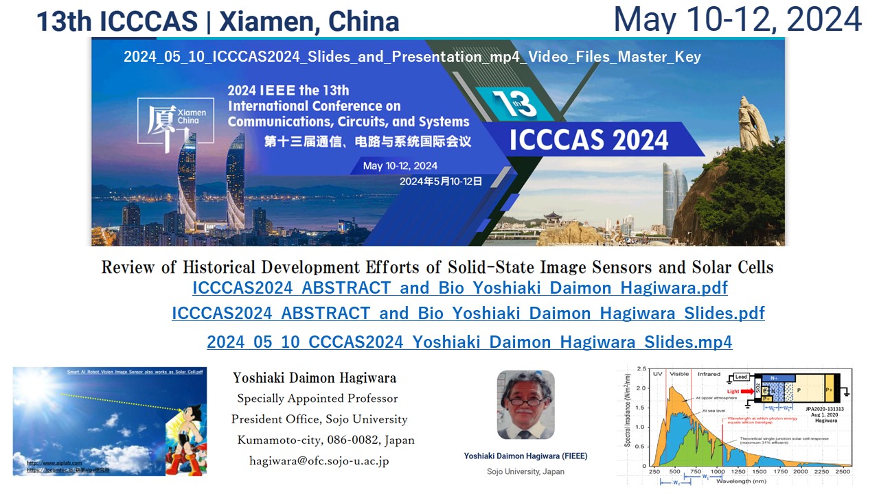
2024_05_10_ICCCAS2024_Slides_and_Presentation_mp4_Video_Files_by_Yoshiaki_Daimon_Hagiwara.pdf
++++++++++++++++++++++++++++++++++++++++++++++++++++++
http://www.icccas.org/
ICCCAS2023_Conference_paper_on_"AIPS_with_Pinned_Buried_Photodiode_used_for_Robot_Vision_and_Solar_Cell_Panel"
++++++++++++++++++++++++++++++++++++++++++++++++++++++
"Chronology_of_Silicon-based_Image_Sensor_development"- Y. D. Hagiwara.pdf
https://eds.ieee.org/images/files/newsletters/Newsletter_Jan23.pdf
is on
IEEE_EDS_Newsletter_January2023_Issue.pdf
https://eds.ieee.org/publications/eds-newsletter
++++++++++++++++++++++++++++++++++++++++++++++++++++++
2024_04_Publication_List_and_Bio_Yoshiaki_Daimon_Hagiwara.pdf
http://www.aiplab.com/
++++++++++++++++++++++++++++++++++++++++++++++++++++++
++++++++++++++++++++++++++++++++++++++++++++++++++++++
Evidence_that_Hagiwara_at_Sony_invented_Pinned_Buried_Photodiode_in_1975.pdf
http://www.aiplab.com/
Yoshiaki_Hagiwara_Bio.pdf
++++++++++++++++++++++++++++++++++++++++++++++++++++++
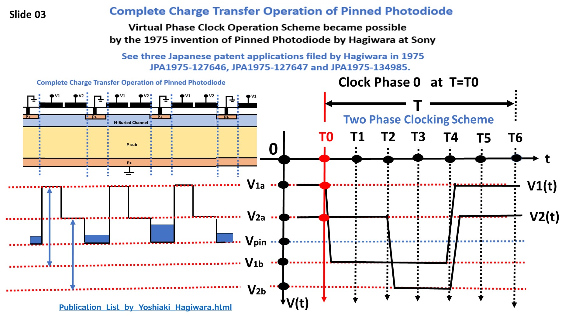
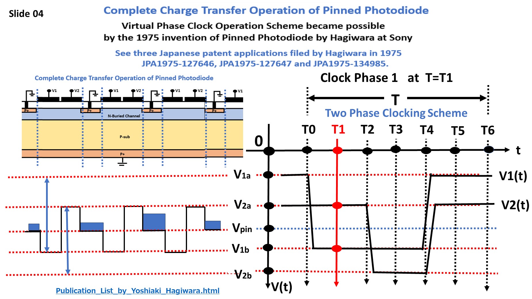
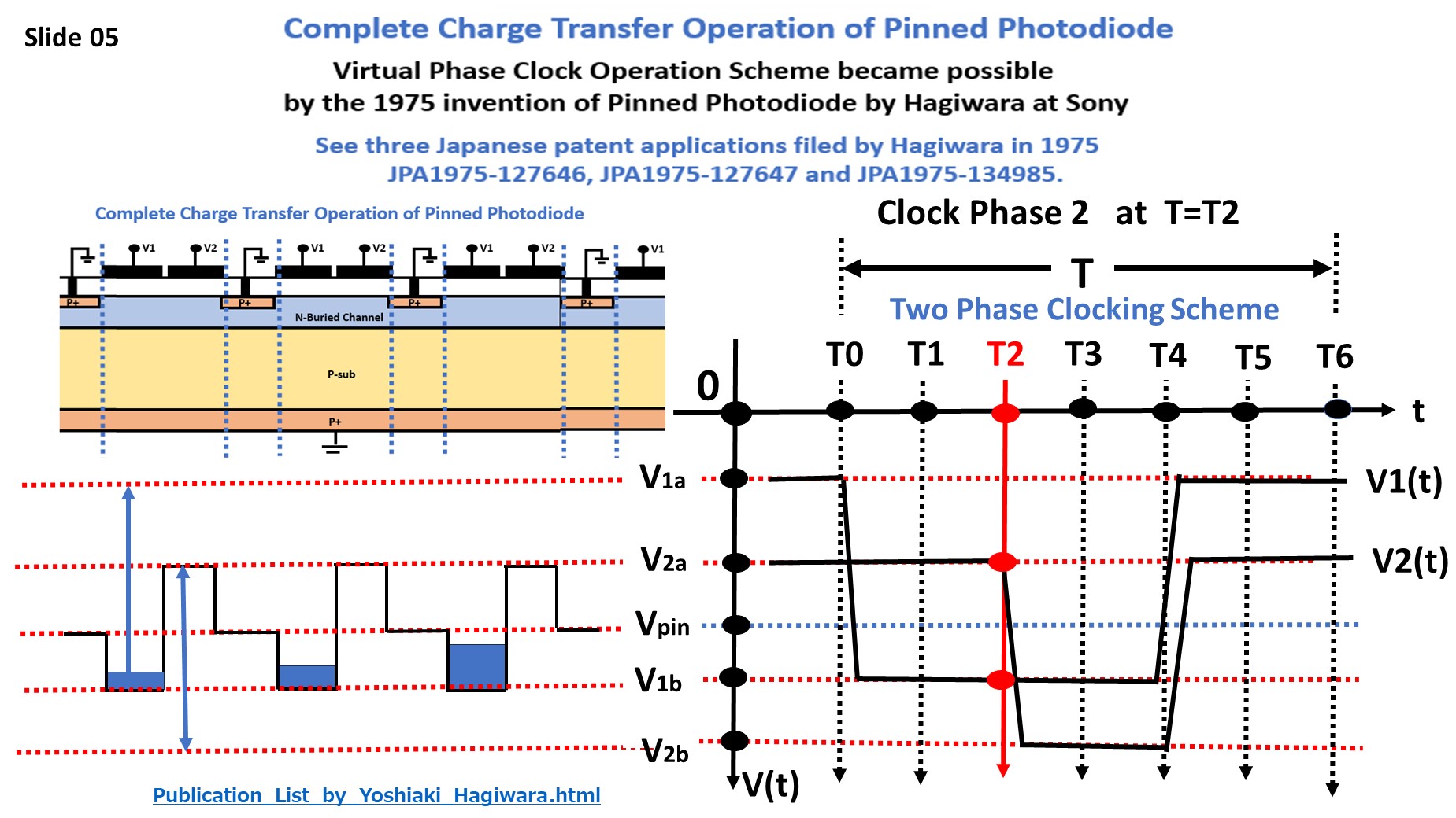
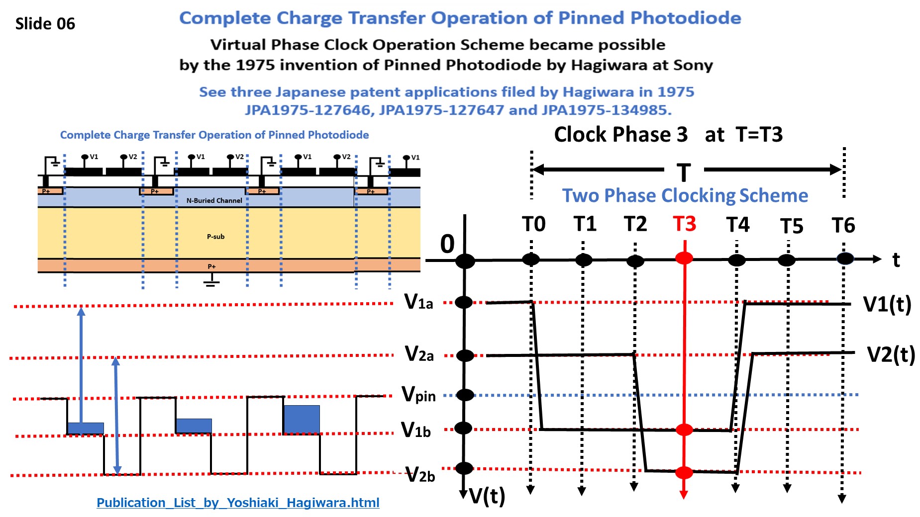
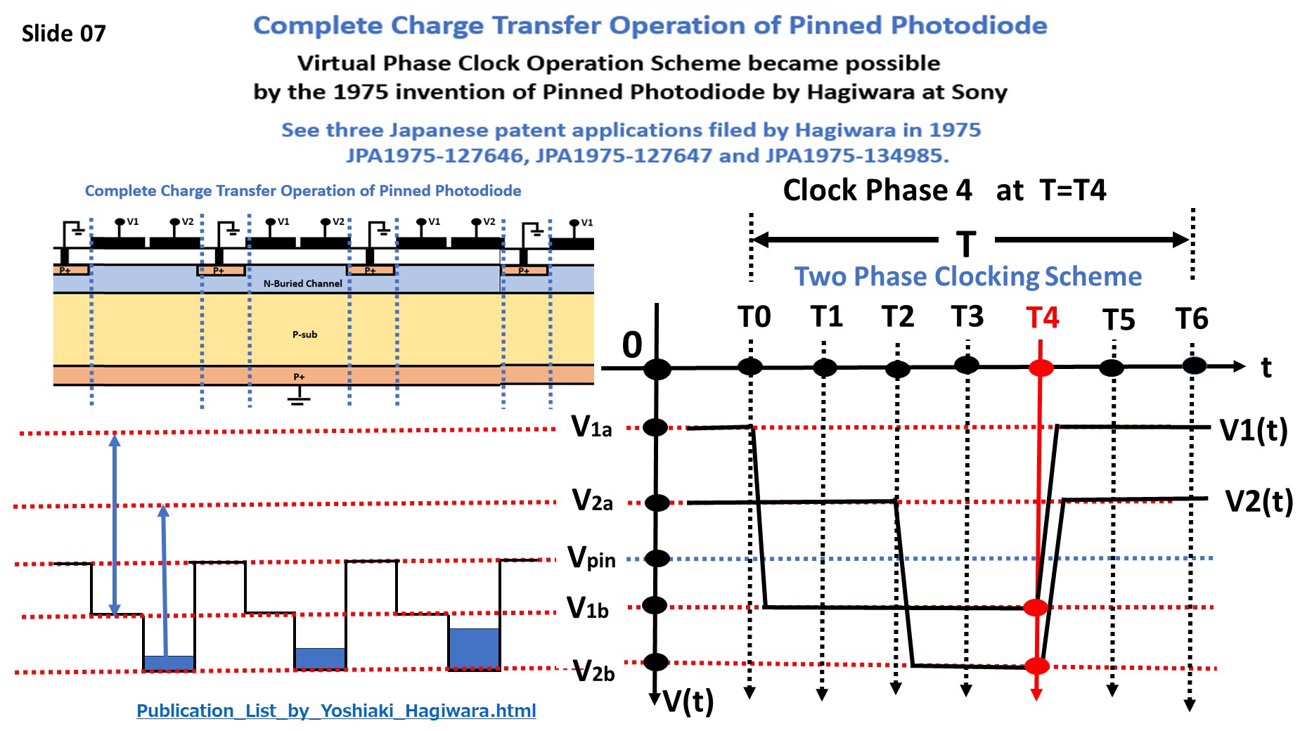
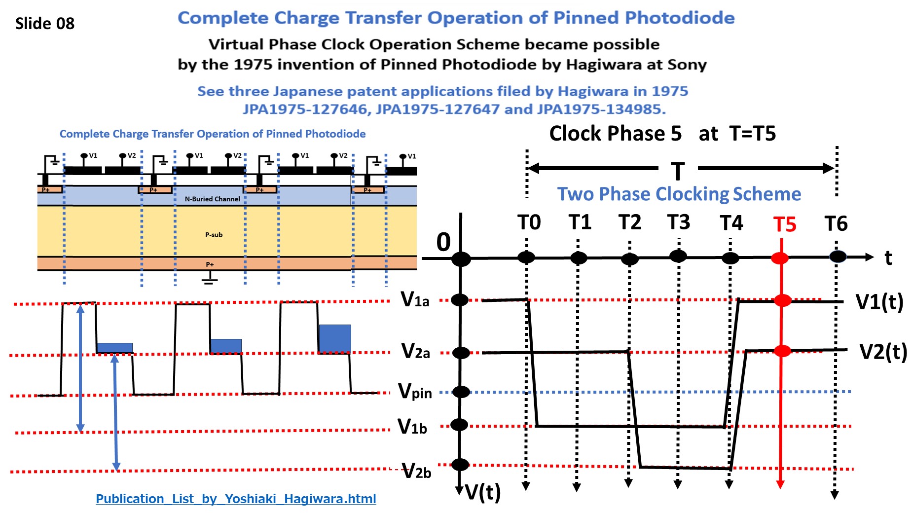
Virtual_Phase_Clock_Operation_Scheme_became_possible
by_Pinned_Photodiode_invented_by_Hagiwara_at_Sony_in_1975_TOP.pdf
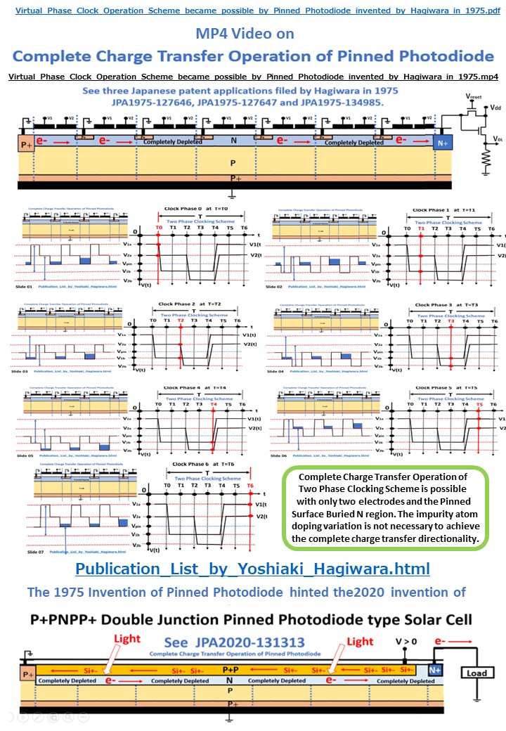
Virtual_Phase_Clock_Operation_Scheme_became_possible
by_Pinned_Photodiode_invented_by_Hagiwara_at_Sony_in_1975.html
slides_pdf.file
++++++++++++++++++++++++++++++++++++++++++++++++++++++
Slide01
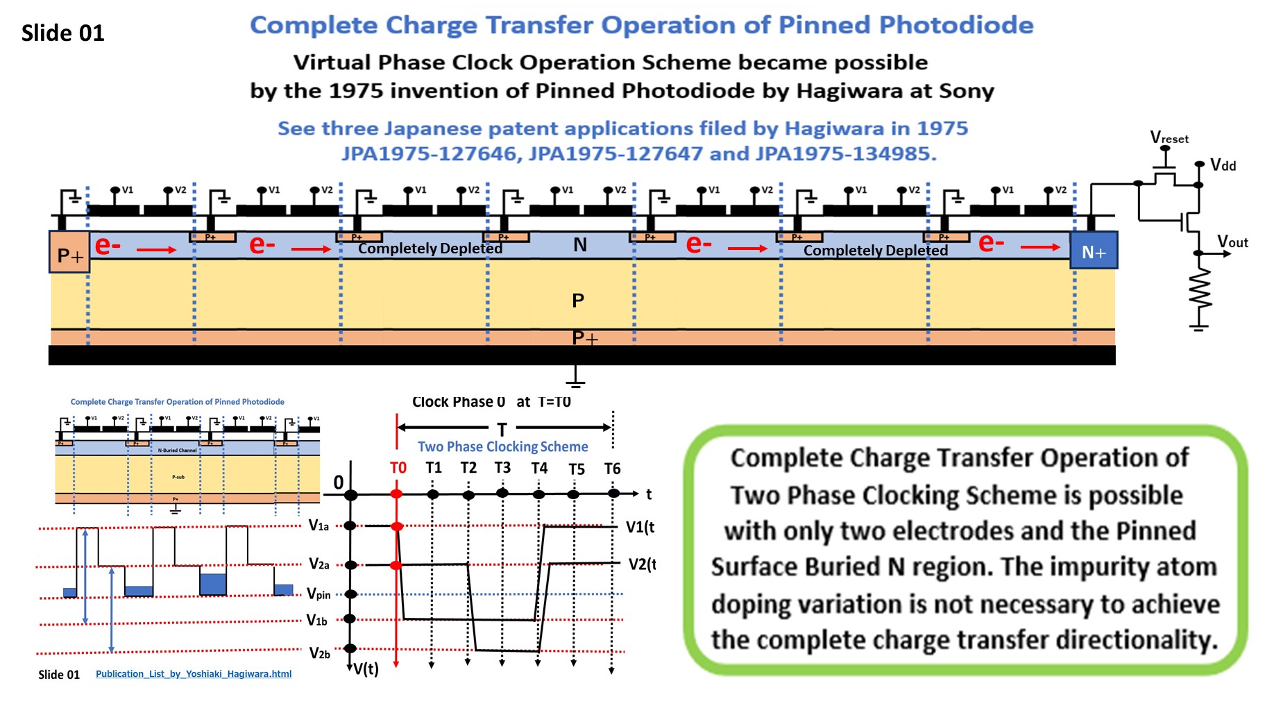
Slide02

Slide03
Slide04
Slide05
Slide06
Slide07
Slide08
Slide09
Slide10
++++++++++++++++++++++++++++++++++++++++++++++++++++++
Recent Publications on Pinned Photodiode
++++++++++++++++++++++++++++++++++++
(R26) P2019_3DIC2019_Paper_on_3D_Pinned_Photodiode_6_pages.pdf
(R27) P2020_EDTM2020_PaperID_3C4_by_Hagiwara_4_pages.pdf
EDTM2020_Paper_on_the P+PN+P Junction Pinned Photodiode and Schottky Barrier Photodiode.html
(R28) P2021_IJSSA2021_Paper_20210616_on_Electrostatic_and_Dynamic_Analysis_of_Pinned_Photodiodes.pdf
P2021_IJSSA2021_Paper_20210616_on_Electrostatic_and_Dynamic_Analysis_of_Pinned_Photodiodes.html
(R29) ICECET2021_Paper61_html
(R30) ICECET2021_Paper75_html
(R31) Chronology_of_Silicon_based_Image_Sensor_Development
IEEE_Electron_Devices_Society_Newsletter_January_2023
++++++++++++++++++++++++++++++++++++
http://www.icecet.com/home
http://www.icecet.com/ICECET_Program.pdf
ICECET2021_Session_E-III_chaired_by_Yoshiaki_Hagiwara.pdf
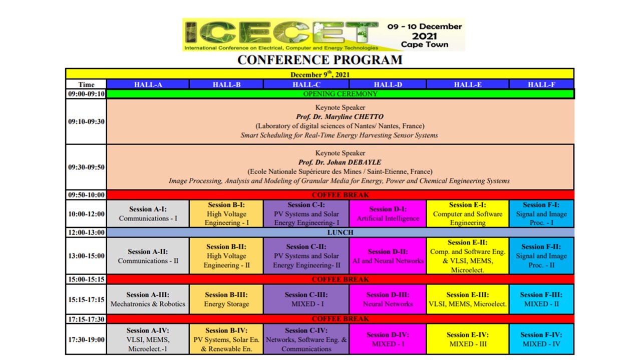
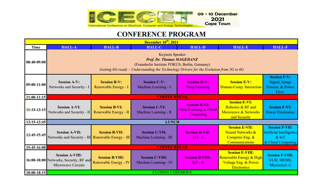
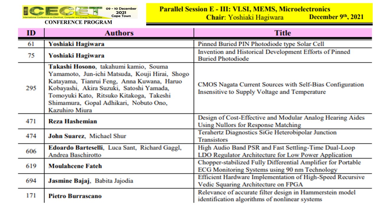
ICECET2021_Program_Session_E-III.pdf
++++++++++++++++++++++++++++++++++++
The presentation slides, pdf, mp3 audio and mp4 video files
of my papers 061 and 075 are now all uploaded into:
(R29) ICECET2021_Paper61_html
(R30) ICECET2021_Paper75_html
held at the IEEE ICECET2021 conference
in Cape Town, South Afrrica on Dec 9 and 10, 2021.
http://www.icecet.com/home
http://www.icecet.com/ICECET_Program.pdf
ICECET2021_Session_E-III_chaired_by_Yoshiaki_Hagiwara.pdf
*************************************************************
001A_ICECET2021_Paper061_Pinned Buried PIN Photodiode type Solar Cell.pdf
001B_ICECET2021_acceptance_letter_ID_061.pdf
001C_ICECET 2021_PARTICIPATION_CERTIFICATE_061.pdf
001D_ICECET2021_Paper061_supplement_Process_Flow_of_Pinned_Buried_PIN_Photodiode_type_Solar_Cell_2021_08_14.pdf
002A_ICECET2021_Paper075_Invention and Historical Development Efforts of Pinned Buried Photodiode.pdf
002B_ICECET2021_acceptance_letter_ID_075.pdf
002C_ICECET 2021 PARTICIPATION CERTIFICATE_075.pdf
002D_ICECET2021_Paper075_supplement_The_Evidence_that_Hagiwar_at_Sony_invente_Pinne_Burie_Photodiode_in_1975.pdf
003_ICECET2021_CHAIR_CERTIFICATE_Session_E3.pdf
004_ICECET2001_Session_E-III_Chaired_by_Yoshiaki_Hagiwara.pdf
*************************************************************
++++++++++++++++++++++++++++++++++++
A Japanese Newspaper by Sangyou Times
wrote an aticle on Hagiwara Profile.
on Nov 13, 2020
++++++++++++++++++++++++++++++++++++
https://www.sangyo-times.jp/article.aspx?ID=5331
Sangyo-Times.jp/article_ID=5331_(PDF)
Sangyo-Times.jp/article_ID=5331_(html)
++++++++++++++++++++++++++++++++++++
Pinned_Buried_Photodiode_with_Electrical_Shutter_Function.pdf
++++++++++++++++++++++++++++++++++++
(P001)April 1973
"The Influence of Interface States on Incomplete Charge Transfer in Overlapping Gate Charge Coupled Devices"
IEEE Journal of Solid State Circuits,Vol. SC 8, No.2, April 1973
(P002)February 1974
"Charge Transfer of Buried Channel Charge Coupled Devices"
Proceeding of International Solid State Circuit Conference
(ISSCC1974),San Francisco, February 1974.
(P003)April 1974
"Final Stage of the Charge Transfer Process in Charge Coupled Devices"
IEEE Transactions on Electron Devices, Vol. ED-21, No.4, April 1974
(P004)June 1975
Caltech_1975_PhD_Thesis_by_Yoshiaki_Daimon_Hagihara.pdf
in Electrical Engineering (major) and Physics(minor), June 1975,
California Institute of Technology, Pasadena, California USA.
(P005) October 23,1975
Japanese Patent Application JPA1975-127646
on "Back-light Triple Junction Type Pinned Buried Photodiode
with Complete Charge Transfer Capability and Global Shutter Fucntion",
Japanese PAtent Application written in Japanese, filed on Oct 23, 1975
(P006)October 23,1975
Japanese Patent Application JPA1975-127647
on "Back-light Double Junction Type Pinned Buried Photodiode
with Complete Charge Transfer Capability and Global Shutter Function",
Japanese Patent Application written in Japanese, filed on Oct 23, 1975
(P007) November 10 1975
Japanese Patent Application JPA1975-134985
on "Triple Junction Type Pinned Buried Photodiode
with Complete Charge Transfer Capability and
Vertical Overflow Drain Function",Japanese Patent Application
written in Japanese, filed on Nov 10, 1975.
(P008) September 1976
"128-Bit Multi Comparator"
IEEE Journal of Solid State Circuits, VOL.SC11, No.4, October 1976.
(P009) September 1977
P1977_Narrow_Cahnnel_Transfer_Gate_CCD_SSDM1977_Paper_by_Hagiwara.pdf"
Proceeding of the 9th Conference on Solid State Devices,Tokyo, September 1977
(P010) September 1977
Japanese Patent Application JPA1977-126885
on "Electric Shutter Clocking and Gamma Control Scheme
using Overflow Drain (OFD) controlled by Strong Punch Thru OFD Voltage Control",
Japanese Patent Application written in Japanese,filed on Sep 29, 1977
(P011) September 1978
Hagiwara_SSDM1978_Paper_on_Pinned_Buried_Photodiode.pdf
Proceeding of the 10th Conference on Solid State Devices,Tokyo, September 1978.
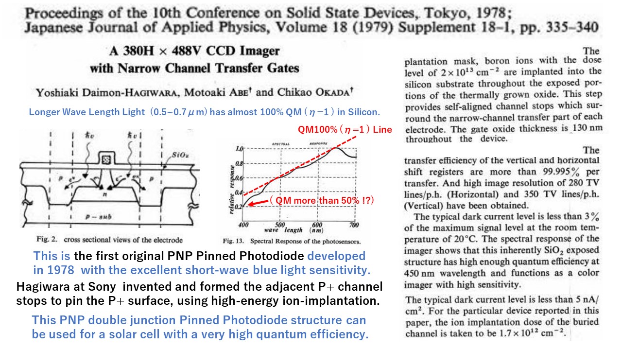
P1978_SSDM1978_Paper_on_the_double_junction_type_Pinned_Photodiode.pdf
(P012) September 1979
"ADVANCES in CCD Imager " Technical Digest of IEEE International Conference
of CCD Image Sensors (IEEE CCD'79),Edinburgh, Scotland UK, September 1979.
(P013) May 1980
IEEE ECS1980 invited paper on "A CCD color imager with narrow-channel transfer gates"
Proceeding of the 157th Electrochemical Society Meeting, May 11-16, 1980, St. Luis, USA.
(P014) November 1980
Technology Book on "CCD Image Sensor and Applications" Trickeps Press, November 1980.
(P015) October 1989
"A 25-ns 4-Mbit CMOS SRAM with Dynamic Bit-Line Loads"
IEEE Journal of Solid State Circuits, vol.24, no.5, October 1989.
(P016) December 1996
IEEE1996_Review_Paper_on_Sony_1980_One_Chip_FT_CCD_Image_Sensor
with_Pinned_Buried_Photodiode
IEEE Transaction on electron Devices, VOl.43, No.12, Dec 1996.
(P017) November 1997
"Sony Semiconductor History"
Addressed at the 23th Research Seminar
in Tokyo Communication University, Nov 28, 1997.
(P018) November 1998
"DRAM/SRAM Technology and Problem.pdf"
Proceedings of the Institute of Electrostatics Japan,
127 Vol. 22 No. 6, 1998, pp.177-178.
(P019) September 2001
"Micro-Electronics for Home Entertainment"
an invited ESSCIRC2001 Plenary Talk,
Technical Digest of IEEE ESSCIRC2001 International Conference (ESSCIRC2001),
Villach, Austria, September, 2001.
(P020) December 2004
Turorial Short Cource on Image Sesnors by Yoshiaki Hagiwara.pdf
IEEE IEDM2004 Conference Short Course at IEDM2004 Short Course, December 2004.
++++++++++++++++++++++++++++++++
(P021) May 2004
++++++++++++++++++++++++++++++++++++++++++++++++++
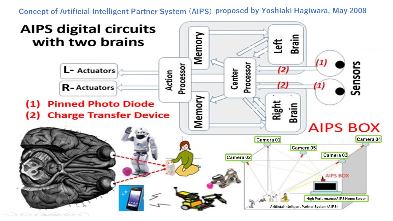
Artificial_Intelligent_Partner_System_AIPS_proposed_by_Yoshiaki_Hagiwara_on_May_2008.pdf
++++++++++++++++++++++++++++++++++++++++++++++++++++++
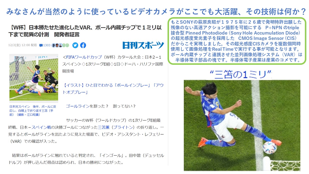
Sensor_Technology_in_World_Cup.pdf
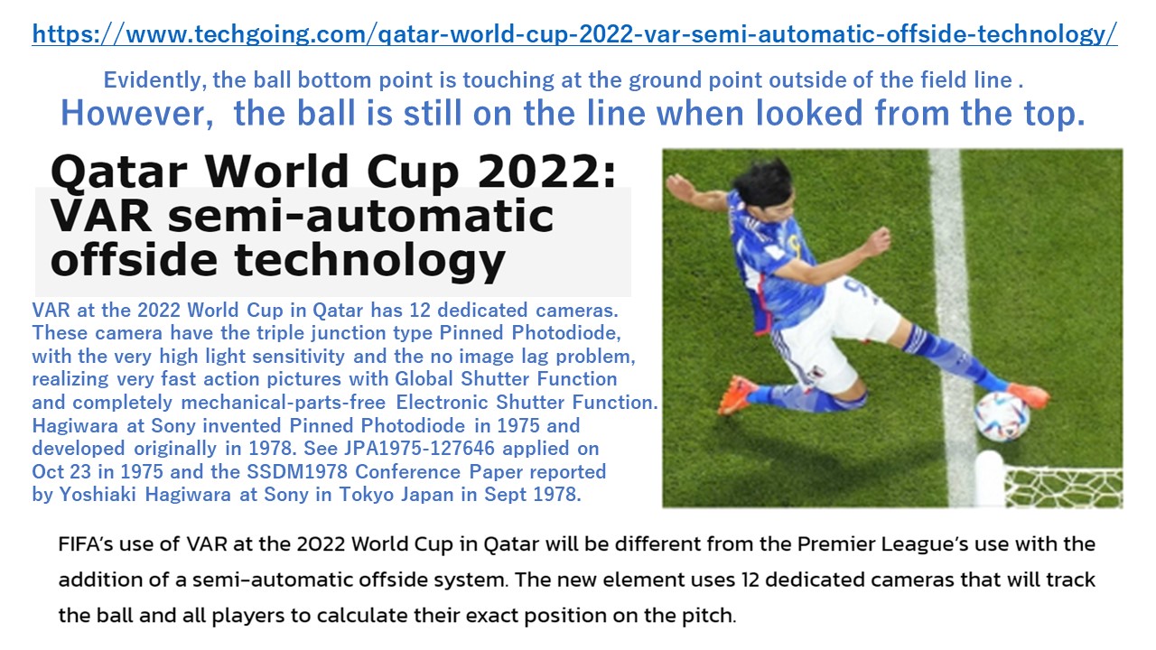
Sony_Sensor_Technology_in_World_Cup.pdf
++++++++++++++++++++++++++++++++++++++++++++++++++++++
(P021A) September 2008
"SOI Design in Cell Processor and Beyond"
an invited ESSCIRC2008 Plenary Talk, Technical Digest of IEEE ESSCIRC2008 Conference,
Edinburgh, Scotland UK, September 2008.
(P021B) December 2008
"Prospect of Developing AIPS Robots for Home Total Supporting Systems"
IEICE technical report, December 12, 2008,ICD2008 Conference, Tokyo, Japan,Vol 108-247, pp.85-90
++++++++++++++++++++++++++++++++++++++++++++++++++++++
(P022) February 2013
Invited Plenary Panel Talk at ISSCCC2013 on Feb. 2013 on Image Sensors
(P023) June 2013
"The p-n-p-n Diode in Future Linear Motor Cars and in Modern Imagers"
IEEE Journal of Solid State Circuits, June issue, 2013.
(P024) July 2014
Japanese Patent Application JPA2014_135497
on "Digital Transformation Matrix for Fast Image Recognition System"
Japanese Patent Application written in Japanese, filed on July 1, 2014.
(P025) July 2014
"Design of Time to Frequency Domain Discrete Fourier Transfer Hardware Engine and its performance estimation"
Digest of Technical Papers at the Japan Electron Society sponsored
Integrated Circuit Workshop ( IEEJ ECT ) in Izumo, Japan, on July 4, 2014.
(P026) June 2015
"Digital Frequency Transformation Circuit for Time-wise Unequally Sampled Data"
THE INSTITUTE OF ELECTRONICS,INFORMATION AND COMMUNICATION ENGINEERS (IEICE) Technical Paper
on June 2015 in Kumamoto-city, Japan.
(P027) April 2017
IEEE_CoolChips_2017_Conference_Invited_Panel_Talk_on_Intelligent_Image_Sensor_Systems.pdf
(P028) October 2019
"Multichip CMOS Image Sensor Structure for Flash Image Acquisition"
IEEE International 3D Systems Integration Conference 2019 (3DIC2019),
Digest of Technical Papers, Sendai, Japan, Paper4017, October 2019.
(P029) March 2020
"Simulation and Device Characterization of the P+PN+P Junction Type Pinned Photodiode and Schottky Barrier Photodiode"
IEEE Electron Device and Manufacturing Technology Conference (EDTM2020),
Digestof Technical Papers, Penang Malaysia, Paper ID 3C4, March 2020.
(P030) August 2020
Japanese Patent Application JPA2020-131313
on "Double Junction Pinned Buried Photodiode Type splar Cell"
Japanese Patent Application written in Japanese,
filed on August 1, 2020.
(P031) June 2021
"Electrostatic and Dynamic Analysis of P+PNP Double Junction Type
and P+PNPN Triple Junction Type Pinned Photodiodes",
International Journal of Systems Science and Applied Mathematics, June 2,
doi: 10.11648/j.ijssam.20210602.13;
ISSN: 2575-5838 (Print);
ISSN: 2575-5803 (Online)
http://www.sciencepublishinggroup.com/journal/paperinfo?journalid=245&doi=10.11648/j.ijssam.20210602.13
(P032) Dec 9 2021 ICECET2021 Paper61
P2021_ICECET2021_Paper61_on_Pinned_Buried_PIN_Photodiode_Type_Solar_Cell.pdf
(P033) Dec 9 2021 ICECET2021 Paper75
P2021_ICECET2021_Paper75_on_Invention_and_Historical_Development_Efforts_of_Pinned_Burie_Photodiode.pdf
(P034) IEEE_Electron_Devices_Society_Newsletter_January_2023
P2023_IEEE_EDS_Newsletter_Jan_2023_on_Chronology_of_Silicon_based_Image_Sensor_Development.pdf
++++++++++++++++++++++++++++++++++++++++++++++++++++
Contributions to International Conferences and Organizations
++++++++++++++++++++++++++++++++++++++++++++++++++++
(C01) International Standardization Committee (1989-1992)
IEC TC47 Technical Committee Chair (1992)
(C02) JEDEC Memory Chips Standardization Committee (2000-2004)
(C03) IEEE EDS ICMTS International Program and Executive Committee (1991-2008)
General Chair (2003-2004);http://icmts.if.t.u-tokyo.ac.jp/home
(C04) IEEE SSS ISSCC Asian Program Committee (2001-2007)
ISSCC Asian Chair (2006-2007);http://isscc.org/
(C05) IEEE SSS ISSCC2008 International Program and Executive Committee (2007-2008)
International Program Chair (2007-2008); http://isscc.org/
(C06) IEEE Computer Society Cool Chips Organization Committee (2001-2010)
https://www.coolchips.org/
(C07) IEEE Computer Society Cool Chips Advisory Committee (2011-2021)
https://www.coolchips.org/
(C08) Visiting Professorship in Electric Engineering Department and
Applied Physics Department at California Institute of Technology,
Pasadena, califor, USA, 1998-1999;https://www.caltech.edu/
(C09) Professorship in Electircal Engineering Department at Gunma University,
Kiryu-city, Gunma-ken, Japan, 2001-2008;https://www.gunma-u.ac.jp/
(C10) Professorship in Information and Communication Tecnology Department
at Sojo University, Kumamoto-city, Japan, 2009-2017; https://www.sojo-u.ac.jp/
(C11) Artificial Intelligent Partner System (AIPS) Consortium,Kanagawa-ken NPO, Japan,
President and CEO (2008-2017); http://www.aiplab.com//
(C12) Society of Semiconductore Industry Experts of Japan ; http://www.ssis.or.jp/
currently also serving as the chairman of the SSIS Education Executive Committee.
+++++++++++++++++++++++++++++++++++++++++++++++++++++++++++++++
List of Realted PDF files decribing the works of Yoshiaki Hagiwara
+++++++++++++++++++++++++++++++++++++++++++++++++++++++++++++++
(R01) Sony_vs_Loral_Patent_War_1_Reviews.pdf
(R02) Sony_vs_Loral_Patent_War_2_Supporting_Opinions.pdf
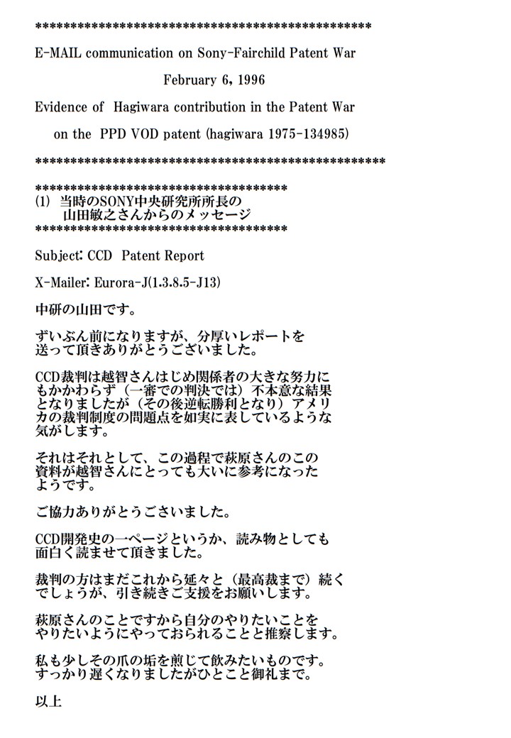
(R03) E-mail_Communication_on_Sony_Loral_Patent_War_1996.pdf
(R04) E-mail_communication_with_Albert_san_2018_07_10.pdf
(R05) HAD_sensor_NEC_SONY_Patent_War.pdf
(R06) JP1980_138026_NEC_Buried_Photodiode_Patent.pdf
(R07) JP1978-1971_Toshiba_Yamada_VOD_patent.pdf
(R08) Sony_vs_Loral_PAtent_War_13_pages.pdf
(R09) Sony_vs_Loral_Patent_War_53_pages.pdf
(R10) Image_Sensor_Story_by_Hagiwara.pdf
(R11) The_evidence_that_Hagiwara_is_the_inventor_of_Pinned_Photodiode_7_pages.pdf
(R12) Future_of_Image_Sensors_and_Solar_Cells.pdf
(R13) JP1975-127646_NPNP_triple_junction_Pinned_Photodiode_Patent_32_pages.pdf
(R14) The_First_Pinned_Photodiode_was_invented_in_1975_by_Yoshiaki_Hagiwar_at_Sony.pdf
(R15) JP1975-127647_NPN_double_junction_Pinned_Photodiode_Patent_22_pages.pdf
(R16) JP1975-134985_PNP_double_junction_Pinned_Photodiode_on_Nsub_Patent_7_pages.pdf
(R17) JP1977-126885_Elecric_Shutter_Clocking_Scheme_by_OFD_Punch_Thru_Action_13_pages.pdf
(R18) JP2014-135497_Digital_Transformation_Circuit_for_Image_Sensors_29_pages.pdf
(R19) JP2020_131313_on_Doubel_Junction_Pinned_Photodiode_Solar_Cell_65_Pages.pdf
(R19A) JPA_2020_131313_Japan_Patent_6818208_on_Pinned_Photodiode_type_Solar_Cell_by_Hagiwara.pdf
(R20) P1978_Pinned_Photodiode_1978_Paper_by_Hagiwara_7_Pages.pdf
(R21) P1996_Pinned_Photodidoe_used_in_Sony_1980_FT_CCD_Image_Sensor_9_Pages.pdf
(R22) P2001_ESSCIRC2001_Micro-Electronics_for_Home_Entertainment_11_pages.pdf
(R23) P2008_ESSCIRC_2008_SOI_Design_in_Cell_Processor_and_Beyond_7_pages.pdf
(R24) P2013_ISSCC2013_Panel_Talk_25_pages.pdf
(R25) P2017_CoolChips_Panel_170419_29_pages.pdf
(R26) P2019_3DIC2019_Paper_on_3D_Pinned_Photodiode_6_pages.pdf
(R27) P2020_EDTM2020_PaperID_3C4_by_Hagiwara_4_pages.pdf
(R28) P2021_IJSSA2021_Paper_20210616_on_Electrostatic_and_Dynamic_Analysis_of_Pinned_Photodiodes.pdf
(R29) ICECET2021_Paper61_html
(R30) ICECET2021_Paper75_html
(R31) Chronology_of_Silicon_based_Image_Sensor_Development
IEEE_Electron_Devices_Society_Newsletter_January_2023
++++++++++++++++++++++++++++++++++++++++++++++++++++++++++++++++++++++
(Q01) Buried_Photodiode_is_not_always_PPD_Hagiwara_Nov_2020.pdf
(Q02) Caltech_1975_PhD_Thesis_Yoshiaki_Daimon_Hagihara.pdf
(Q03) Difference_of_Buried_Photodiode_and_Pinned_Photodiode.pdf
(Q04) E-mail_Communication_on_Sony_Loral_Patent_War_1996.pdf
(Q05) E-mail_communication_with_Albert_and_Yoshi.pdf
(Q06) E-mail_communication_with_Albert_san_2018_07_10.pdf
(Q07) E-mail_communication_with_Albert_san_2018_07_10A.pdf
(Q08) E-mail_communication_with_Albert_san_2018_07_10B.pdf
(Q09) Evidence_that_Hagiwara_is_the_inventor_of_Pinned_Photodiode_2020_10_04a.pdf
(Q10) Evidence_that_Hagiwara_is_the_inventor_of_Pinned_Photodiode_in_Japanese.pdf
+++++++++++++++++++++++++++++++++++++++++++++++++++++++++
+++++++++++++++++++++++++++++++++++++++++++++++++++++++++
Introduction to the world of Digital Circuits for Artificial Intelligence
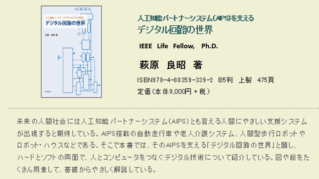
If you are interestied in the book, Please visit
https://www.seizansha.co.jp/ISBN/ISBN978-4-88359-339-2.html
https://www.seizansha.co.jp/
*************************************************************
++++++++++++++++++++++++++++++++++++
A Japanese Newspaper by Sangyou Times
wrote an aticle on Hagiwara Profile.
on Nov 13, 2020
++++++++++++++++++++++++++++++++++++
https://www.sangyo-times.jp/article.aspx?ID=5331
Sangyo-Times.jp/article_ID=5331_(PDF)
Sangyo-Times.jp/article_ID=5331_(html)
++++++++++++++++++++++++++++++++++++
+++++++++++++++++++++++++++++++++++++++++++++++
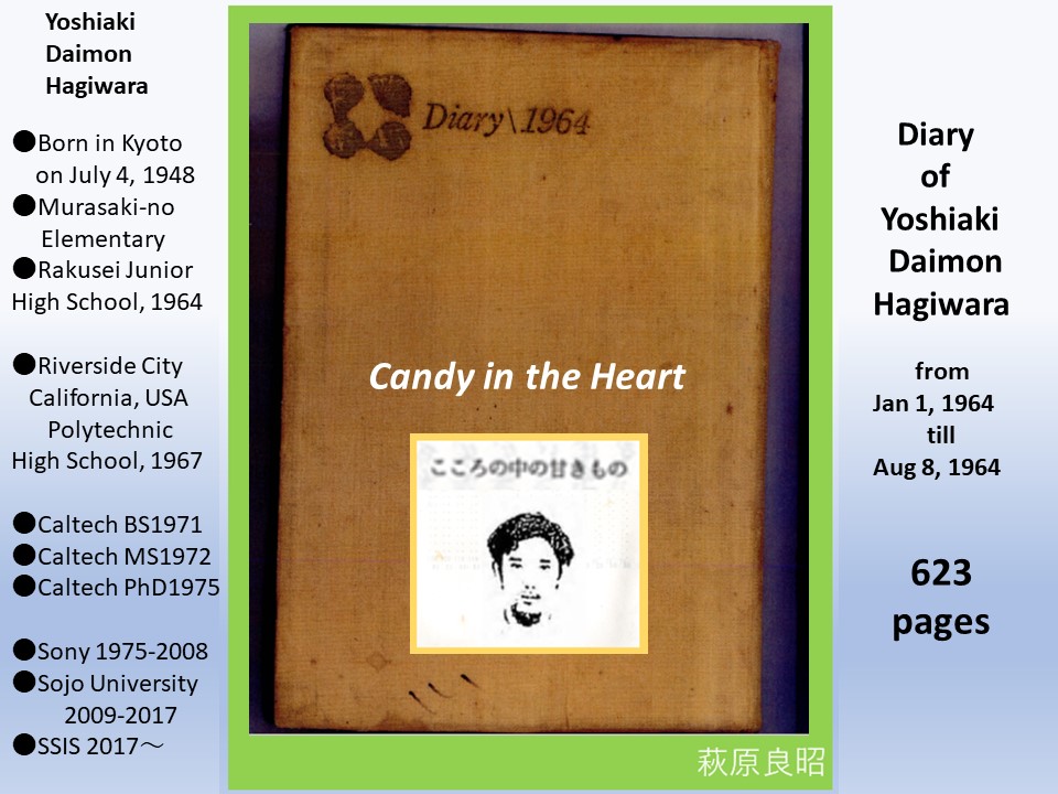
Candty_in_the_Heart.html
こころの中の甘きもの♡
Hagiwara_Yoshiaki_Voice_Diary_in_1964
1964年15歳当時の萩原良昭の日記と音声朗読集
+++++++++++++++++++++++++++++++++++++++++++++++
+++++++++++++++++++++++++++++++++++++++++++
随筆 「Candy in the Heart」 萩原良昭 著
+++++++++++++++++++++++++++++++++++++++++++
中学3年生の正月から高校1年生の日記をエッセイにしたものです。
仮名ですが登場人物はすべて当時実在する人です。
+++++++++++++++++++++++++++++++++++++++++++
Candy_in_the_Heart
Jump to Page
TOP
010,
020,
030,
040,
050,
060,
070,
080,
090,
100
110,
120,
130,
140,
150,
160,
170,
180,
190,
200
210,
220,
230,
240,
250,
260,
270,
280,
290,
300
310,
320,
330,
340,
350,
360,
370,
380,
390,
400
410,
420,
430,
440,
450,
460,
470,
480,
490,
500
510,
520,
530,
540,
550,
560,
570,
580,
590,
600
610,
620
+++++++++++++++++++++++++++++++++++++++++++
++++++++++++++++++++++++++++++++++++++++++++++
2022_06_07_Gunma_Top.html
++++++++++++++++++++++++++++++++++++++++++++++
2022年6月7日(火)群馬大学アナログ集積回路研究会での特別講義の内容のご紹介です
人工知能ロボットを支える、超光感度の賢い電子の目を太陽電池に応用する
++++++++++++++++++++++++++++++++++++++++++++++
++++++++++++++++++++++++++++++++++++++++++++++
Please_Support_Our_Activity.html
++++++++++++++++++++++++++++++++++++++++++++++
国や企業を動かすために新型太陽電池の開発推進活動をご支援していただける有志を多数募集中です
新型太陽電池の開発推進活動をご支援していただける有志を募集案内です
++++++++++++++++++++++++++++++++++++++++++++++
++++++++++++++++++++++++++++++++++++++++++++++
日本の産業のコメとして戦略的に重要な半導体電子部品の基本知識
++++++++++++++++++++++++++++++++++++++++++++++
(0)はじめに
(1)金属と絶縁体の違い
(2)半導体の基本特性
(3)single接合型のダイオードの整流特性
(4)double 接合型バイポーラトランジスタの電流増幅特性
(5)triple 接合型サイリスター型の理想的な高速Switch動作特性
(6)MOS型のトランジスタの電流増幅特性
(7)CMOS型インバータ回路の省エネ特性
(8)超光感度のCMOS型イメージセンサーの特性
(9)P+PNPP+接合の double接合型の新型太陽電池の構造とその動作原理
イメージセンサーと太陽電池の動作原理_萩原良昭.html
+++++++++++++++++++++++++++++++++++++++++++++++++++++++++
超光感度半導体受光素子を太陽電池に使う事に挑戦します_萩原良昭.pdf
++++++++++++++++++++++++++++++++++++++++++++++++++++++
電子デバイス産業新聞2025年1月10日記事「ソニーの快男児、萩原良昭氏は新世代の鉄腕アトムを作る!」
2025_03_03_厚木市発SDGs支援団体_合同会社LOOMTEC社_AIPS萩原研究所の夢を実現に応援をお願いもうしあげます.pdf
01
02
03
04
05
06
07
08
09
10
11
12
13
14
15
16
17
18
19
20
21
22
23
24
25
26
27
28
29
30
31
32
33
34
35
36
37
38
39
40
41
電子デバイス産業新聞2025年1月10日記事「ソニーの快男児、萩原良昭氏は新世代の鉄腕アトムを作る!」
2025_03_03_厚木市発SDGs支援団体_合同会社LOOMTEC社_AIPS萩原研究所の夢を実現に応援をお願いもうしあげます.pdf
++++++++++++++++++++++++++++++++++++++++++++++++++++++
++++++++++++++++++++++++++++++++++++++++++++++++++++++
https://www.caltech.edu/MS1971/BS1972/PhD1975
https://www.ieee.org/IEEE Life Fellow
https://www.sojo-u.ac.jp/崇城大学特任教授
https://www.ssis.or.jp/半導体産業人協会会員
https://ja.wikipedia.org/wiki/萩原良昭
https://en.wikipedia.org/wiki/Yoshiaki_Hagiwara
++++++++++++++++++++++++++++++++++++++++++++++++++++++
+++++++++++++++++++++++++++++++++++++++++++++++++++++++++
Return to Top Home Page of Yoshiaki Hagiwara (AIPS)
http://www.aiplab.com
+++++++++++++++++++++++++++++++++++++++++++++++++++++++++